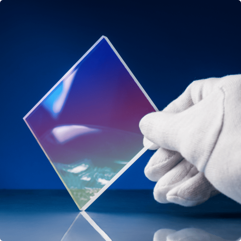
Photonic devices are designed to emit, reflect, transmit, or absorb photons spanning the electromagnetic spectrum from x-rays to the far infrared and have features ranging in size from nanoscale to tens of microns. All this is possible with materials as diverse as indium phosphide (InP), gallium nitride (GaN), silicon-based dielectrics, metals such as gold and platinum, and lithium niobate (LiNbO3). There isn’t any part of life that doesn’t use or rely on photonic devices. Whether for illumination, optotelecommunication, sensing, or displays, photonics is playing the critical role.
Most photonics devices are built using compound semiconductor materials, an area of manufacturing for which Plasma-Therm® is well known. When you partner with us, you’ll be tapping into the expertise that comes from installing more than 1,300 systems in both R&D and production.
Etch
Whether your photonics devices need high temperature for InP etching or ion-beam etching for lithium niobate or low-damage etching for microLEDs, we have it.
Wafer Clean
Our high-density radical flux (HDRF™) low-temperature, downstream technology is proven for photonics applications, including photoresist removal without ion exposure, for optimum-quality devices.
Plasma Dicing
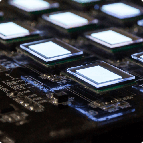
Plasma dicing with the Singulator® system is ideal for damage-sensitive photonics devices. You get smooth sidewalls, improved die strength, street sizes <10µm, and any shape die you want.
Photonics Applications


Explore All Process Technology
We continuously improve our plasma etch, deposition, and dicing technology to help you build the best products on the market.
NEED ASSISTANCE?
Let our experts help you customize our processes solutions for your applications.