Dicing Without Tape
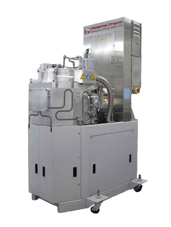
PDOC avoids using etching systems without tape and tape frames. The wafers on the carriers are loaded using standard approaches, such as SMIF (standard mechanical interface) pods. Processes such as lithography or resist strip can be done at a wafer level without the complications of tape and tape frames. Once the wafer is diced, the die are transferred back to the dicing tape and tape frame, where they can undergo the next packaging steps.
All the benefits of plasma dicing are realized, with narrower streets, no microcracking from saws or heat-affected areas from lasers, and faster singulation times.
Tape Frames
PDOC does not use tape frames for the plasma etching step, allowing for conventional wafer-handling approaches.
Wafer Level Processing
With wafer on carrier, other processes such as lithography or metallization can be done without tape frames.
After Grinding
With thin and ultra-thin wafers, plasma dicing is done from the front side of wafers after backside grinding, maintaining the simple process flow used with saw dicing.
OUR PDOC PRODUCTS
EXPLORE TECHNICAL PAPERS
Want to learn more about this topic? Click here to review technical papers on PDOT principles, practices and outcomes.
SEE ALL SINGULATION PRODUCTS
To review all our singulation products, processes, capabilities, and brands, click here.
NEED ASSISTANCE?
Let our experts help you customize our processes solutions for your applications.

