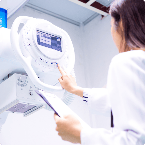
The digital transformation is here, powered by a plethora of microelectromechanical systems (MEMS) and sensors. From mobile and wearable consumer devices to automotive, medical, and industrial Internet of Things (IIOT) applications, MEMS and sensors are critical for capturing data that is processed to inform our actions.
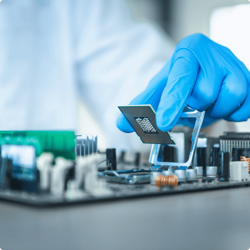
MEMS fabrication is not standardized and spans a variety of technology areas, including electronics, fluidics, mechanics, magnetics, acoustics, and optics. Each unique design can require many different etch, deposition, and release steps. Our platforms are the centerpiece of our process technologies and cover a wide variety of applications, including etch, deposition, strip, material modification, and singulation.
Etch
Our equipment and processes for deep silicon and oxide etching let you create features in silicon and SOI with vertical, high aspect ratios.
Deposition
We’ve fine-tuned an array of plasma-enhanced deposition processes to help you achieve the film features you need for optimal device performance.
Sacrificial Layer Removal and PR Strip
Our unique high-density radical flux (HDRF™) technology offers stiction-free release of structures and gentle removal of PR masks.
MEMS & Sensor Applications

EXPLORE ALL PROCESS TECHNOLOGY
We continuously improve our plasma etch, deposition, and dicing technology to help you build the best products on the market.
NEED ASSISTANCE?
Let our experts help you customize our processes solutions for your applications.